
Silicon Tetraiodide
Silicon tetraiodide (also known as silicon iodide, tetraiodo silane, silane, silicon (IV) iodide) is a tetrahedral molecule with the chemical formula of SiI4. SiI4 is a light, colorless and moisture sensitive crystalline structure. When melted, SiI4 appears as a yellow liquid. SiI4 is commonly used in the manufacturing and etching in microelectronics and is a precursor molecule to silicon amides. The following table summarizes the chemical properties of silicon tetraiodide:
Chemical Properties |
|
| Molecular Weight (Da) | 535.7034 |
| Appearance | white |
| Melting Point | 120.5 °C, 394 K, 249 °F |
| Boiling Point | 287.4 °C, 561 K, 549 °F |
| Density | 4.198 g/cm3 |
| Storage | Dry, well-ventilated |
| Sensitivity | Light, air and moisture |
| Incompatibilities | Magnesium, zinc, ammonia, aluminum |
SiI4
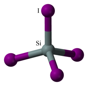
SiI4 is formed as iodine vapor and carbon dioxide is passed over strongly-heated silicon. It is at this step that the iodo compound condenses in the cold portion of the condenser and is subsequently purified by shaking with mercury and carbon bisulphide. The resultant crystallization structure is octahedral, with a melting point of 120.5°C and boiling point at 287.4°C. The SiI4 vapor burns as a red flame. Silicon iodoform, SiHI3, is a result of the addition of hydriodic acid on silicon, for which the resultant product contains silicon tetraiodide. Downstream fractionation is needed to separate the resulting compounds.
Reagent Use
Silicon tetraiodide has been the interest of chemists in the manufacturing of microchips. SiI4 is a starting chemical for the manufacturing and etching of silicon wafers used in microfabrication of electronic related components. Etching is the process of chemically removing wafer layers during the manufacturing process. The etching process is critical to the process and all silicon wafers undergo multiple etching steps. Briefly, the parts of the wafer to not be etched are protected from the etchant by a masking material that resists etching. The known etch rates of etchants allow precise control of the depth of the cavity.
Silicon
Silicon (symbol Si; atomic weight 28.08) is a crystalline solid exhibiting a blue-grey metallic face. With the exception of oxygen, silicon is the most abundant of all elements, but rarely occurs as the pure element. Silicon is found in the form of anhydrous or hydrated oxide (silica), such as quartz, sand, tridymite, opal, but it also occurs in the form of silicates of magnesium, aluminum and iron. It is also found in alkaline earth metals forming various soils and rocks, along with numerous parts of plants and in the stars in the sky.
Silicon exists in two forms, amorphous and crystalline. Raw silicon is always contaminated with impurities and methods used for the preparation of amorphous silicon do not give good results (by decomposition of silicofluorides or silicon halides). There are methods to produce a pure variety of silicon by heating silicon with aluminum. Amorphous silicon appearance is a brown colored powder. The crystalline form of silicon can be prepared following a variety of published procedures, such as heating potassium silicofluoride with aluminum. Crystalline silicon appearance is grey in color, but can vary depending on preparation method.
In the semiconductor world, silicon and germanium are the primary elements used as a result of having four electrons available in its outer orbit structure. This structure enables the formation of a precise lattice by covalent bonds with four adjacent atoms. In addition, the resulting molecules contain an innate property that enables the incorporation of impurities. The added impurities modify the conductive electronic properties of the molecule such that conductivity of the resultant material can be fine-tuned and controlled.
Silicon Dopants
Silicon in its purest form is not a valuable element at conducting electricity. However, by slightly altering the molecular composition of the semiconductor, or doping the crystalline structure with other elements, the resultant compound now becomes a useful and controllable conductor. Semiconductor dopants typically consist of trivalent or pentavalent elements, depending on the semiconductor type desired. As their name implies, trivalent elements contain three electrons in their outer shell, whereas pentavalent elements contain five electrons in their outer shell. Using a tri- or pentavalent element as a dopant in creation of a semiconductor results in a crystalline structure with very different electrical properties. Trivalent dopants do not have enough free electrons to bond with four elements, so an electron deficiency or P-type semiconductor is created. Conversely, pentavalent dopants have an extra electron in the outer shell when bound to four elements, so the extra electron is free to move about in the crystalline structure and is called an N-type semiconductor.
Whether the semiconductor dopant creates a P-type or N-type semiconductor, electrical current still flows for similar reasons as any other conductor whereas negative charges push electrons and positive charges push electrons. However, the purpose of contaminating crystalline silicon to create P-type or N-type semiconductors is to increase conductivity as much as 1 x 10⁶ by the addition of very little dopants. Impurity ranges of dopants include 1 impurity per 1,000 silicon atoms up to 1 impurity per 1 x 10⁹ silicon atoms.
Iodine
Iodine (symbol I; atomic weight 126.90), is a solid exhibiting a metallic grey color at standard conditions and belongs to the halogen group of elements. However, iodine readily sublimes to form a violet colored gas. Iodine is not found in nature in the uncombined state but rather as a diatomic molecule.
Iodine volatilizes slowly at temperatures ordinary to surface temperature. However, upon heating, iodine quickly volatilizes and the gaseous color passes from violet to a deep indigo blue. The resultant color change as a vapor exhibits that iodine molecules become structurally less complex as temperature increases.
Although iodine has a distinctive smell it is not as pungent as that of other halogens such as chlorine or bromine. Solubility in water is minimal, but iodine readily dissolves in alcohols, chloroform, hydrocarbons and alkaline iodide solutions. Also, although chemical properties of iodine closely resemble bromine and chlorine, it exhibits much less binding affinity to other elements.
Historically, the ashes of seaweed was the main source of iodine. Large heaps of seaweed were burnt, taking care to monitor temperature in order to control volatilization of iodine. This initial collection step can be varied by boiling seaweed in large vats containing sodium carbonate. The extracts of any of these methods is separated into soluble and insoluble parts. The soluble fraction is concentrated and eventually distilled to obtain the iodine fraction. Currently, hot brines from gas fields are the main source of iodine and follow a controlled extraction process.
Unlike other halogens that are routinely used in industrial applications, iodine has more distinct rather than broad uses. Iodine is commonly used in supplements for animal feed, dyes/pigments, sanitation, photography and catalysts. There are reports of iodine used for cloud seeding and smog inhibition. Iodine applications in chemical reactions are common, but kinetics are slower than other halogens and there formation of hyriodic acid must be overcome.
The Future of Silicon Semiconductors
As engineers push the boundaries of silicon semiconductors in our phones, watches and computer, fundamental limits are reached. With the limitation of purified starting materials removed from the equation, new formulation science will have to push the technology into new territories. One of these areas includes the use of silicon in solar panels and light energy capture. As we all know, sunlight can be captured by semiconductors and turned into an electrical current. Conversely, semiconductors can be used to convert electrical current into the light emission of LED lights and lasers.
Although it is an abundant, accessible, easy to purify and an extremely strong material, the ability of silicon to convert light into electrical signal is very inefficient. Typical efficiency of a silicon solar panel is 10-15% light conversion. New semiconductor materials are being tested that vastly improve the efficiency of light conversion into electricity. These new semiconductors including crystalline structures of antimonides, bismuthides and gallium-nitride are more efficient but become cost prohibitive to manufacture. With this information, engineers are continually experimenting with ways to alter silicon semiconductor properties that would enable them to capture and emit light at a higher efficiency. This will potentially be accomplished by doping the crystalline semiconductor structure with alternate elemental groups not commonly used.
Tetraiodosilane Use in Research
-
- Preparation of silica nanoparticles using silicon tetrachloride for reinforcement of PU. Z. Luo, X. Cai, R.Y. Hong, L.S. Wang, W.G. Feng. Chemical Engineering Journal. Vol 187, 1 April 2012, 357–366.
- Silica nanoparticles were made by hydrolysis of silicon tetrachloride. Tetraiodo silane was the starting material due to its low cost. Silica powders were dispersed in a polyurethane coating which improved the mechanical properties of silica films.
- Preparation of silica nanoparticles using silicon tetrachloride for reinforcement of PU. Z. Luo, X. Cai, R.Y. Hong, L.S. Wang, W.G. Feng. Chemical Engineering Journal. Vol 187, 1 April 2012, 357–366.